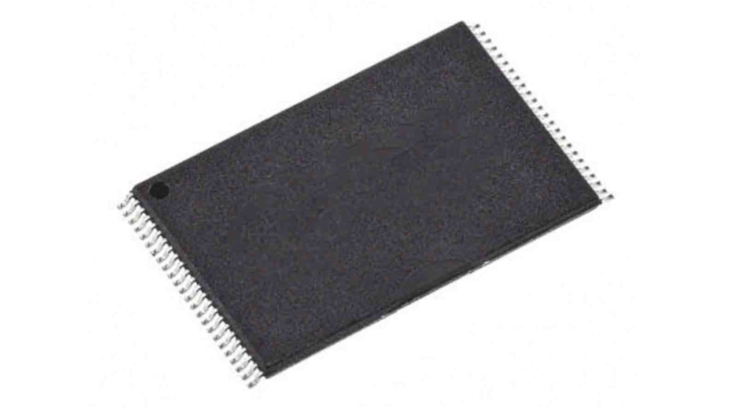
Infineon NOR 16Mbit CFI Flash Memory 48-Pin TSOP, S29AL016J70TFI013

- RS庫存編號:
- 193-8787
- 製造零件編號:
- S29AL016J70TFI013
- 製造商:
- Infineon
985 現貨庫存,可於3工作日發貨。
已增加
單價 个(每托盘 5 )
HK$21.08
| 單位 | Per unit | Per Pack* |
| 5 - 245 | HK$21.08 | HK$105.40 |
| 250 - 495 | HK$20.616 | HK$103.08 |
| 500 + | HK$20.174 | HK$100.87 |
| * 參考價格 | ||
- RS庫存編號:
- 193-8787
- 製造零件編號:
- S29AL016J70TFI013
- 製造商:
- Infineon
產品概覽和技術數據資料表
法例與合規
- COO (Country of Origin):
- TH
產品詳細資訊
The S29AL016J is a 16 Mbit, 3.0 Volt-only Flash memory organized as 2,097,152 bytes or 1,048,576 words. The device is offered in 48-ball Fine-pitch BGA (0.8 mm pitch), 64-ball Fortified BGA (1.0 mm pitch) and 48pin TSOP packages. The word-wide data (x16)appears on DQ15–DQ0, the byte-wide (x8) data appears on DQ7–DQ0. This device is designed to be programmed in-system with the standard system 3.0 volt VCC supply. A 12.0 V VPP or 5.0 VCC are not required for write or erase operations. The device can also be programmed in standard EPROM programmers.
The device offers access time of 55 ns allowing high speed microprocessors to operate without wait states. To eliminate bus contention the device has separate chip enable (CE#), write enable (WE#) and output enable (OE#) controls.
Device programming occurs by executing the program command sequence. This initiates the Embedded Program algorithm an internal algorithm that automatically times the program pulse widths and verifies proper cell margin. The Unlock Bypass mode facilitates faster programming times by requiring only two write cycles to program data instead of four.
Device erasure occurs by executing the erase command sequence. This initiates the Embedded Erase algorithm an internal algorithm that automatically preprograms the array (if it is not already programmed) before executing the erase operation. During erase, the device automatically times the erase pulse widths and verifies proper cell margin. The host system can detect whether a program or erase operation is complete by observing the RY/BY# pin, or by reading the DQ7(Data# Polling) and DQ6 (toggle) status bits. After a program or erase cycle has been completed, the device is ready to read array data or accept another command.
For products that are Customized and under Non-cancellable & Non-returnable, Sales & Conditions apply.
規格
Attribute | Value |
|---|---|
| Memory Size | 16Mbit |
| Interface Type | CFI |
| Package Type | TSOP |
| Pin Count | 48 |
| Organisation | 2M x 8 bit |
| Mounting Type | Surface Mount |
| Cell Type | NOR |
| Minimum Operating Supply Voltage | 2.7 V |
| Maximum Operating Supply Voltage | 3.6 V |
| Block Organisation | Asymmetrical |
| Length | 12mm |
| Height | 1.05mm |
| Width | 18.4mm |
| Dimensions | 18.4 x 12 x 1.05mm |
| Maximum Random Access Time | 70ns |
| Series | S29AL |
| Automotive Standard | AEC-Q100 |
| Minimum Operating Temperature | -40 °C |
| Number of Words | 2M |
| Number of Bits per Word | 8bit |
| Maximum Operating Temperature | +85 °C |