Altera FPGA 5CEBA4 49000 Cells, 49000 Gates, 3464192 bit 18480 Blocks, 256-Pin FBGA
- RS庫存編號:
- 170-2989
- 製造零件編號:
- 5CEBA4F17C8N
- 製造商:
- Altera

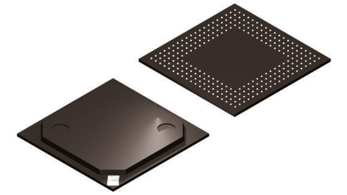
此圖片僅供參考,請參閲產品詳細資訊及規格
可享批量折扣
查看批量定價選項小計(1 托盤,共 90 件)*
HK$74,088.63
訂單超過 HK$250.00 免費送貨
有庫存
- 90 件準備從其他地點送貨
**需要更多嗎?**輸入您需要的數量,然後按一下「查看送貨日期」以查詢更多庫存和送貨詳細資訊。
單位 | 每單位 | 每托盤* |
|---|---|---|
| 90 - 90 | HK$823.207 | HK$74,088.63 |
| 180 - 270 | HK$806.741 | HK$72,606.69 |
| 360 + | HK$790.608 | HK$71,154.72 |
* 參考價格
- RS庫存編號:
- 170-2989
- 製造零件編號:
- 5CEBA4F17C8N
- 製造商:
- Altera
規格
產品概覽和技術數據資料表
法例與合規
產品詳細資訊
透過選取一個或多個屬性來查找類似產品。
選取全部 | 屬性 | 值 |
|---|---|---|
| 品牌 | Altera | |
| Product Type | FPGA | |
| Series | 5CEBA4 | |
| Number of Logic Gates | 49000 | |
| Number of Logic Cells | 49000 | |
| Number of Logic Units | 18480 | |
| Number of Registers | 73920 | |
| Number of Multipliers | 132 | |
| Mount Type | Surface | |
| Minimum Supply Voltage | 1.07V | |
| Package Type | FBGA | |
| Maximum Supply Voltage | 1.13V | |
| Pin Count | 256 | |
| Minimum Operating Temperature | 0°C | |
| Number of RAM Bits | 3464192bit | |
| Maximum Operating Temperature | 85°C | |
| Standards/Approvals | No | |
| Length | 17mm | |
| Automotive Standard | No | |
| 選取全部 | ||
|---|---|---|
品牌 Altera | ||
Product Type FPGA | ||
Series 5CEBA4 | ||
Number of Logic Gates 49000 | ||
Number of Logic Cells 49000 | ||
Number of Logic Units 18480 | ||
Number of Registers 73920 | ||
Number of Multipliers 132 | ||
Mount Type Surface | ||
Minimum Supply Voltage 1.07V | ||
Package Type FBGA | ||
Maximum Supply Voltage 1.13V | ||
Pin Count 256 | ||
Minimum Operating Temperature 0°C | ||
Number of RAM Bits 3464192bit | ||
Maximum Operating Temperature 85°C | ||
Standards/Approvals No | ||
Length 17mm | ||
Automotive Standard No | ||
- COO (Country of Origin):
- US
Cyclone FPGA, Altera
An FPGA is a semiconductor device consisting of a Matrix of Configurable Logic Blocks (CLBs) connected through programmable interconnects. The user determines these interconnections by programming SRAM. A CLB can be simple (AND, OR gates, etc) or complex (a Block of RAM). The FPGA allows changes to be MADE to a design even after the device is soldered into a PCB.
相关链接
- Altera FPGA 5CEBA4F17C8N 5CEBA4 49000 Cells 3464192 bit 18480 Blocks, 256-Pin FBGA
- Altera FPGA Cyclone III 15408 Cells 484-Pin FBGA
- Altera FPGA Cyclone III 55856 Cells 484-Pin FBGA
- Altera FPGA Cyclone IV 28848 Cells 484-Pin FBGA
- Altera FPGA 5CEBA2 25000 Cells 2002944 bit 9434 Blocks, 256-Pin FBGA
- Altera FPGA 5CEBA2F17C8N 5CEBA2 25000 Cells 2002944 bit 9434 Blocks, 256-Pin FBGA
- Altera FPGA EP4CGX15BF14C8N Cyclone IV GX 14400 Cells 169-Pin FBGA
- Altera FPGA Cyclone IV E 6272 Cells 276480 bit 392 Blocks, 256-Pin FBGA