Nexperia 74LVC1G86GW,125 2-Input XOR Logic Gate, 5-Pin TSSOP
- RS庫存編號:
- 152-3698
- 製造零件編號:
- 74LVC1G86GW,125
- 製造商:
- Nexperia

可享批量折扣
小計(1 包,共 100 件)*
HK$43.70
訂單超過 HK$250.00 免費送貨
有庫存
- 5,400 件準備從其他地點送貨
**需要更多嗎?**輸入您需要的數量,然後按一下「查看送貨日期」以查詢更多庫存和送貨詳細資訊。
單位 | 每單位 | 每包* |
|---|---|---|
| 100 - 700 | HK$0.437 | HK$43.70 |
| 800 - 1400 | HK$0.426 | HK$42.60 |
| 1500 + | HK$0.42 | HK$42.00 |
* 參考價格
- RS庫存編號:
- 152-3698
- 製造零件編號:
- 74LVC1G86GW,125
- 製造商:
- Nexperia
規格
產品概覽和技術數據資料表
法例與合規
產品詳細資訊
透過選取一個或多個屬性來查找類似產品。
選取全部 | 屬性 | 值 |
|---|---|---|
| 品牌 | Nexperia | |
| Logic Function | XOR | |
| Mounting Type | Surface Mount | |
| Number of Elements | 1 | |
| Number of Inputs per Gate | 2 | |
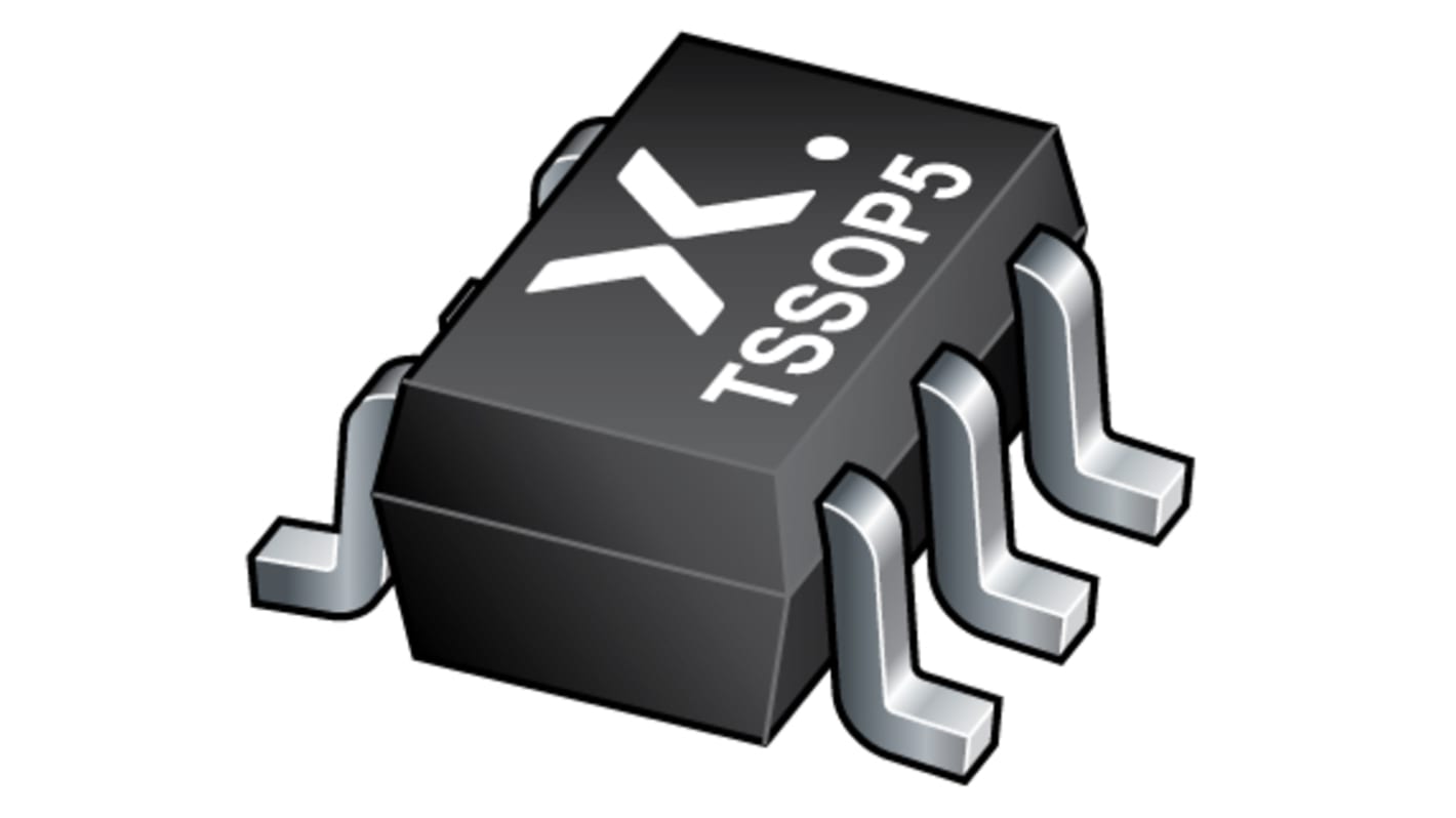
| Package Type | TSSOP | |
| Pin Count | 5 | |
| Logic Family | 74LVC | |
| Input Type | CMOS | |
| Maximum Operating Supply Voltage | 5.5 V | |
| Maximum Propagation Delay Time @ Maximum CL | 13 ns @ 50 pF | |
| Minimum Operating Supply Voltage | 1.65 V | |
| Propagation Delay Test Condition | 50pF | |
| Minimum Operating Temperature | -40 °C | |
| Dimensions | 2.25 x 1.35 x 1mm | |
| Width | 1.35mm | |
| Length | 2.25mm | |
| Height | 1mm | |
| Maximum Operating Temperature | +125 °C | |
| 選取全部 | ||
|---|---|---|
品牌 Nexperia | ||
Logic Function XOR | ||
Mounting Type Surface Mount | ||
Number of Elements 1 | ||
Number of Inputs per Gate 2 | ||
Package Type TSSOP | ||
Pin Count 5 | ||
Logic Family 74LVC | ||
Input Type CMOS | ||
Maximum Operating Supply Voltage 5.5 V | ||
Maximum Propagation Delay Time @ Maximum CL 13 ns @ 50 pF | ||
Minimum Operating Supply Voltage 1.65 V | ||
Propagation Delay Test Condition 50pF | ||
Minimum Operating Temperature -40 °C | ||
Dimensions 2.25 x 1.35 x 1mm | ||
Width 1.35mm | ||
Length 2.25mm | ||
Height 1mm | ||
Maximum Operating Temperature +125 °C | ||
2-input EXCLUSIVE-OR gate, The 74LVC1G86 provides the 2-input EXCLUSIVE-OR function. Inputs can be driven from either 3.3 V or 5 V devices. These features allow the use of these devices in a mixed 3.3 V and 5 V environment. This device is fully specified for partial Power-down applications using IOFF. The IOFF circuitry disables the output, preventing the damaging backflow current through the device when it is powered down.
Wide supply voltage range from 1.65 V to 5.5 V
High noise immunity
CMOS low power consumption
Latch-up performance exceeds 250 mA
Direct interface with TTL levels
Inputs accept voltages up to 5 V
Multiple package options
High noise immunity
CMOS low power consumption
Latch-up performance exceeds 250 mA
Direct interface with TTL levels
Inputs accept voltages up to 5 V
Multiple package options