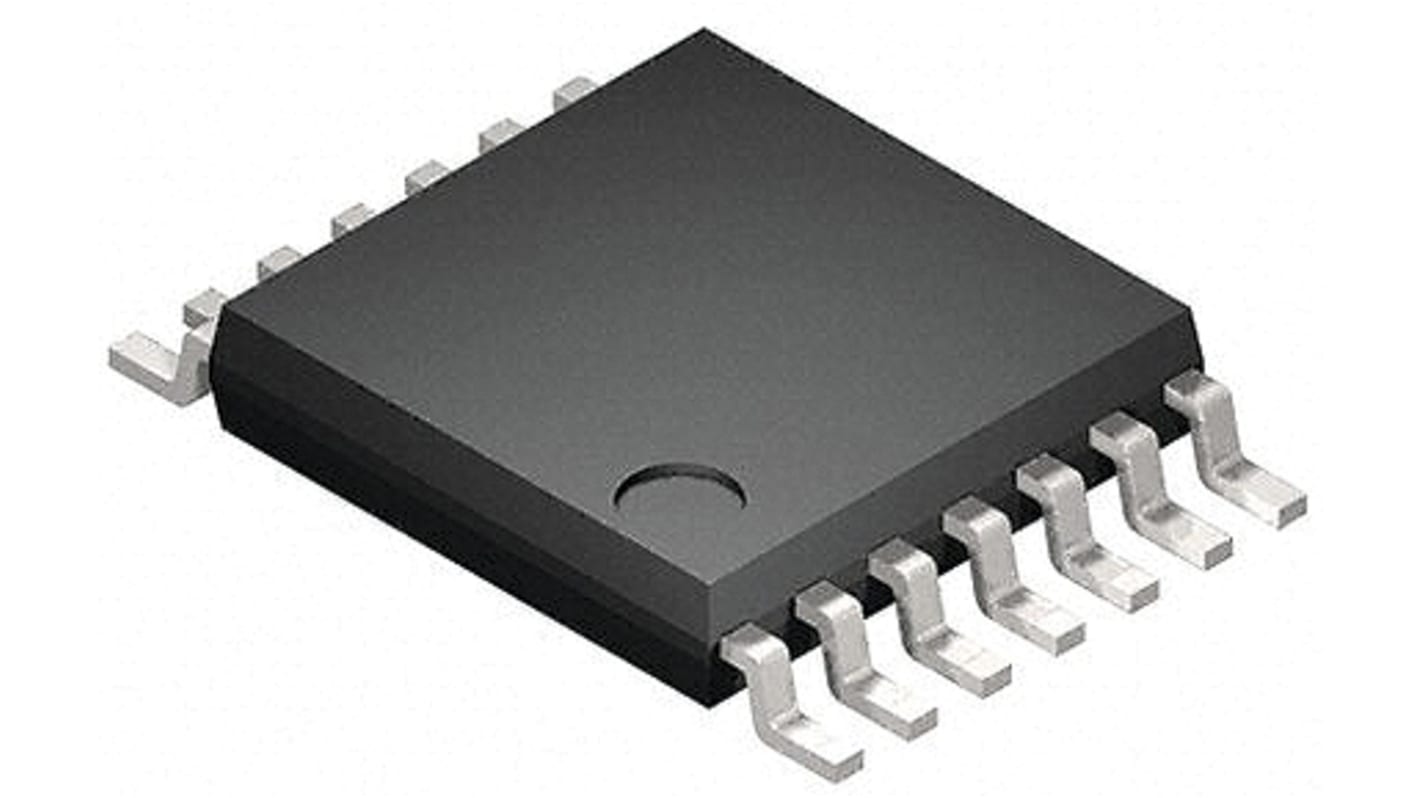
Toshiba 74VHC20FT, Dual 4-Input NAND Logic Gate, 14-Pin TSSOP
- RS庫存編號:
- 171-3421
- 製造零件編號:
- 74VHC20FT
- 製造商:
- Toshiba

小計(1 包,共 50 件)*
HK$49.20
訂單超過 HK$250.00 免費送貨
最後的 RS 庫存
- 最終 1,600 個,準備發貨
單位 | 每單位 | 每包* |
|---|---|---|
| 50 + | HK$0.984 | HK$49.20 |
* 參考價格
- RS庫存編號:
- 171-3421
- 製造零件編號:
- 74VHC20FT
- 製造商:
- Toshiba
規格
產品概覽和技術數據資料表
法例與合規
產品詳細資訊
透過選取一個或多個屬性來查找類似產品。
選取全部 | 屬性 | 值 |
|---|---|---|
| 品牌 | Toshiba | |
| Logic Function | NAND | |
| Mounting Type | Surface Mount | |
| Number of Elements | 2 | |
| Number of Inputs per Gate | 4 | |
| Package Type | TSSOP | |
| Pin Count | 14 | |
| Logic Family | 74VHC | |
| Input Type | CMOS, TTL | |
| Maximum Operating Supply Voltage | 5.5 V | |
| Maximum High Level Output Current | -8mA | |
| Maximum Propagation Delay Time @ Maximum CL | 13 ns @ 50 pF | |
| Minimum Operating Supply Voltage | 2 V | |
| Maximum Low Level Output Current | 8mA | |
| Height | 1mm | |
| Width | 4.4mm | |
| Dimensions | 5 x 4.4 x 1mm | |
| Minimum Operating Temperature | -40 °C | |
| Automotive Standard | AEC-Q100 | |
| Propagation Delay Test Condition | 50pF | |
| Output Type | Buffer, CMOS | |
| Length | 5mm | |
| Maximum Operating Temperature | +125 °C | |
| 選取全部 | ||
|---|---|---|
品牌 Toshiba | ||
Logic Function NAND | ||
Mounting Type Surface Mount | ||
Number of Elements 2 | ||
Number of Inputs per Gate 4 | ||
Package Type TSSOP | ||
Pin Count 14 | ||
Logic Family 74VHC | ||
Input Type CMOS, TTL | ||
Maximum Operating Supply Voltage 5.5 V | ||
Maximum High Level Output Current -8mA | ||
Maximum Propagation Delay Time @ Maximum CL 13 ns @ 50 pF | ||
Minimum Operating Supply Voltage 2 V | ||
Maximum Low Level Output Current 8mA | ||
Height 1mm | ||
Width 4.4mm | ||
Dimensions 5 x 4.4 x 1mm | ||
Minimum Operating Temperature -40 °C | ||
Automotive Standard AEC-Q100 | ||
Propagation Delay Test Condition 50pF | ||
Output Type Buffer, CMOS | ||
Length 5mm | ||
Maximum Operating Temperature +125 °C | ||
The 74VHC20FT is an advanced high speed CMOS 4-INPUT NAND GATE fabricated with silicon gate C2MOS technology. It achieves the high speed operation similar to equivalent Bipolar Schottky TTL while maintaining the CMOS low power dissipation. The internal circuit is composed of 3 stages including a buffer output, which provide high noise immunity and stable output. An input protection circuit ensures that 0 to 5.5 V can be applied to the input pins without regard to the supply voltage. This device can be used to interface 5 V to 3 V systems and two supply systems such as battery back up. This circuit prevents device destruction due to mismatched supply and input voltages.
Wide operating temperature: Topr = -40 to 125
High speed: tpd = 3.3 ns (typ.) at VCC = 5.0 V
Low power dissipation: ICC = 2.0 μA (max) at Ta = 25
High noise immunity: VNIH = VNIL = 28 % VCC (min)
Power down protection is provided on all inputs.
Balanced propagation delays: tPLH ≈ tPHL
Wide operating voltage range: VCC(opr) = 2.0 V to 5.5 V
Pin and function compatible with the 74 series (AC/HC/AHC/LV etc.) 20 type