Altera DK-DEV-2AGX125N

- RS庫存編號:
- 761-4637
- 製造零件編號:
- DK-DEV-2AGX125N
- 製造商:
- Altera
此產品已停售
- RS庫存編號:
- 761-4637
- 製造零件編號:
- DK-DEV-2AGX125N
- 製造商:
- Altera
產品概覽和技術數據資料表
法例與合規
產品詳細資訊
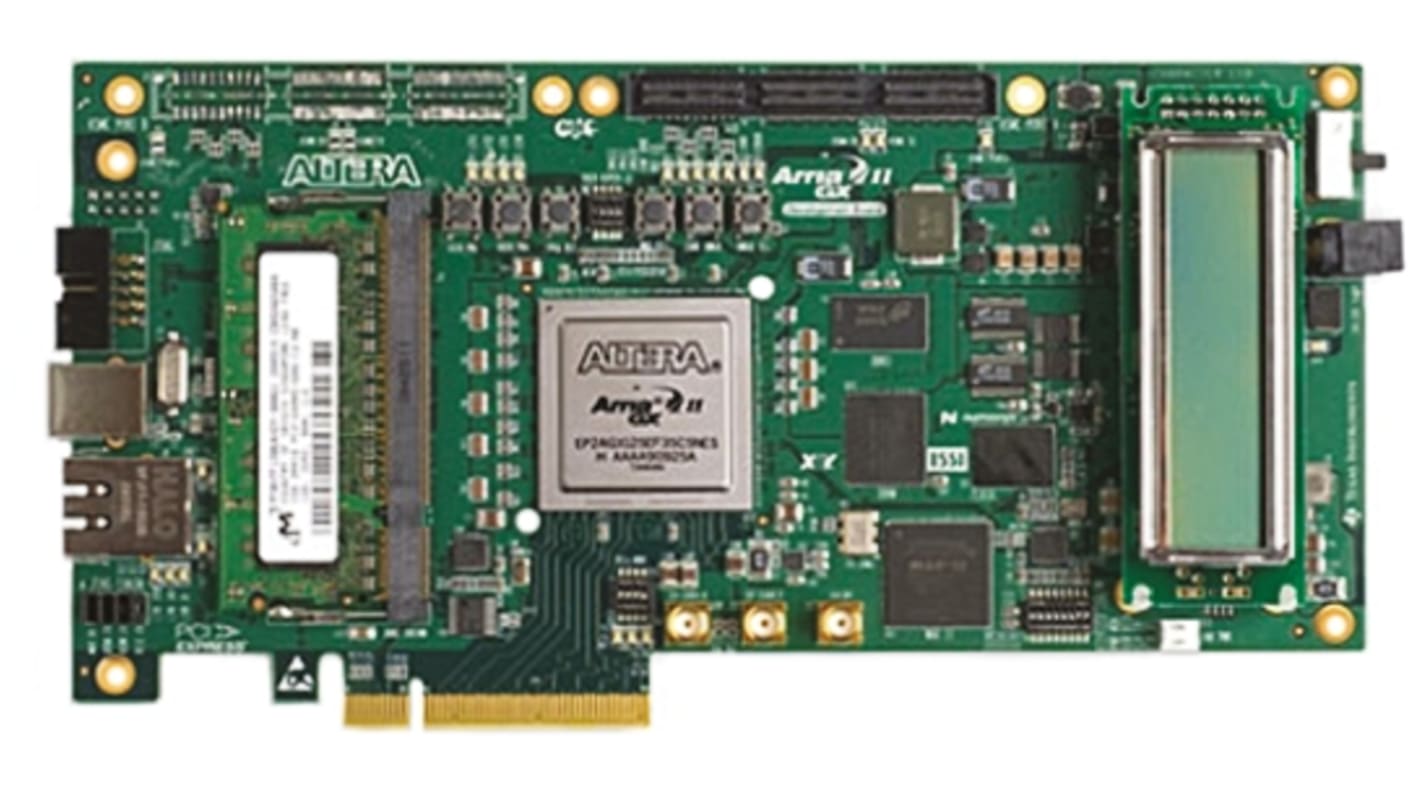
Arria II GX FPGA Development Kit, Altera
The Altera Arria II GX FPGA Development Kit is a complete design environment that includes both the hardware and software you need to develop Arria II GX FPGA designs.
Develop and test PCI Express (PCIe) designs
Develop and test memory subsystems consisting of DDR2 and DDR3 memories
High-speed mezzanine card (HSMC) connectors to interface to over 30 different HSMCs
Supported protocols: 10Gigabit Ethernet, SONET, Common Public Radio Interface (CPRI), Open Base Station Architecture Initiative (OBSAI) and others
Supplied with
USB cable, Ethernet cable, HSMC loopback board, HSMC debug breakout board, Quartus II software, MegaCore IP library & NIOS II Embedded Design Suite.
An FPGA is a semiconductor device consisting of a matrix of Configurable Logic Blocks (CLBs) connected through programmable interconnects. The user determines these interconnections by programming SRAM. A CLB can be simple (AND, OR gates, etc) or complex (a block of RAM). The FPGA allows changes to be made to a design even after the device is soldered into a PCB.
規格
Attribute | Value |
|---|---|
| Classification | Development Kit |
| Technology | FPGA |